


BTS52001ENAXUMA1 PROFET+ 12V Smart High-Side Power Switch Technical Guide
Product Technical Guide BTS52001ENAXUMA1 PROFET+ 12V Smart High-Side Power Switch Technical GuideInfineon Technologies single-channel automotive smart high-side power switch featuring 5V to 28V operati…
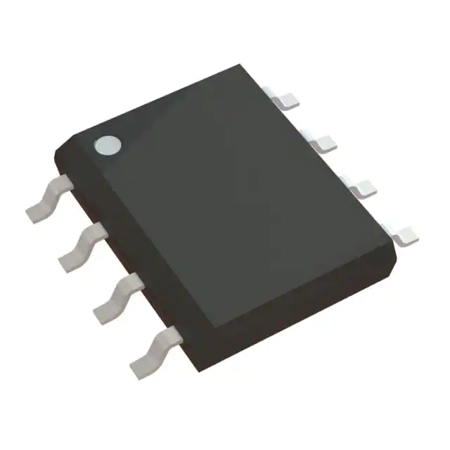
- Part No.:
- BTS52001ENAXUMA1
- Manufacturer:
- Infineon Technologies
- Package:
- 8-SOIC (0.154", 3.90mm Width) Exposed Pad
- Datasheet:
- BTS52001ENAXUMA1.pdf
- Description:
- IC SWITCH PWR HISIDE 8DSO
- Quantity:
-
Original Supply
Strict supplier screening and quality control support.
-
Datasheet Support
Help engineers quickly verify product specifications.
-
BOM Sourcing
Support multi-part procurement and RFQ matching.
BTS52001ENAXUMA1 PROFET+ 12V Smart High-Side Power Switch Technical Guide
Infineon Technologies single-channel automotive smart high-side power switch featuring 5V to 28V operation, 1.5A nominal load current, 200mΩ typical on-resistance, integrated protection, and analog current-sense diagnostics.
Product Introduction
The BTS52001ENAXUMA1 is a single-channel smart high-side power switch manufactured by Infineon Technologies. It belongs to the PROFET™+ 12V family and is designed to control electrical loads connected to automotive low-voltage power systems.
The device combines an N-channel power MOSFET with integrated control, protection, and diagnostic circuitry. Unlike a conventional discrete MOSFET, it can monitor load conditions and respond to electrical faults without requiring a completely separate protection circuit.
The BTS5200-1ENA is designed for a nominal load current of up to 1.5A. Its typical on-state resistance is 200mΩ at a junction temperature of 25°C, increasing to a specified maximum of 400mΩ at 150°C.
The recommended operating supply voltage range is 5V to 28V, making the device suitable for 12V automotive electrical architectures and other compatible DC systems.
The high-side configuration places the switching MOSFET between the positive supply and the electrical load. This allows the load to remain connected to ground while its positive supply is electronically controlled.
Integrated diagnostic functionality includes a dedicated diagnostic-enable input and a current-sense output. The sense output can be connected to a microcontroller analog-to-digital converter to monitor load current and detect selected fault conditions.
The BTS52001ENAXUMA1 is available in an 8-pin PG-TDSO-8-31 surface-mount package with an exposed supply-connected cooling tab.
Typical applications include automotive lighting, small actuators, resistive loads, relay replacement, and electronic power-distribution modules.
Key Benefits
Integrated High-Side Switching
Controls positive supply delivery to loads without requiring a discrete MOSFET gate-driver circuit.
Intelligent Fault Protection
Integrated overload, overtemperature, and other protection functions improve robustness during abnormal load conditions.
Current-Sense Diagnostics
Dedicated diagnostic pins enable microcontroller-based load-current monitoring and fault detection.
Automotive Power Control
Designed for automotive 12V electrical environments and compatible resistive, inductive, and capacitive loads.
Features
- Single-channel smart high-side power switch
- Infineon PROFET™+ 12V product family
- Integrated N-channel power MOSFET
- Nominal load current of 1.5A
- 200mΩ typical on-state resistance at 25°C
- 400mΩ maximum on-state resistance at 150°C
- 5V to 28V recommended supply operating range
- Logic-compatible input control
- Integrated current-limitation function
- Overload and short-circuit protection
- Overtemperature protection
- Overvoltage protection functions
- Inductive-load switching capability within specified energy limits
- Analog load-current sensing
- Diagnostic-enable input
- Open-load detection capability
- Protection and diagnostic functionality for automotive power distribution
- Single power output channel
- Three internally connected output pins
- Supply connection through exposed cooling tab
- PG-TDSO-8-31 surface-mount package
- Specified junction temperature range of -40°C to +150°C
- Tape-and-reel ordering configuration
Design Note: The device's 1.5A nominal load rating must not be confused with its internal short-circuit current-limitation threshold. The latter is a protection characteristic rather than a continuous operating-current rating.
Package
The BTS52001ENAXUMA1 is supplied in Infineon's PG-TDSO-8-31 package, an eight-pin thermally enhanced surface-mount configuration.
- Package Type: PG-TDSO-8-31
- Package Family: Thermally enhanced SO-8
- Pin Count: 8
- Mounting Type: Surface Mount
- Cooling Tab: Electrically connected to VS
- Power Output Connections: Pins 6, 7, and 8
- Product Family: PROFET™+ 12V
- Packaging: Tape and Reel
- Ordering Number: BTS52001ENAXUMA1
The exposed cooling tab is not a ground connection. It is connected internally to the positive supply terminal, VS.
This distinction is critical for PCB design. Connecting the cooling tab to a grounded thermal pad would create an incorrect supply connection and could damage the device or surrounding circuitry.
All three OUT pins must be connected together on the PCB. Output copper width, thermal vias, and the available cooling area should be designed for the expected current and power dissipation.
Use the official Infineon PG-TDSO-8-31 package drawing for the exact mechanical dimensions, solder footprint, assembly clearances, and thermal layout.
Pinout
The BTS52001ENAXUMA1 provides separate logic control, diagnostic control, current sensing, ground, and protected power-output connections.
| Pin | Signal | Function |
|---|---|---|
| 1 | GND | Ground connection for the internal control circuitry. |
| 2 | IN | Input signal controlling activation of the high-side switch. |
| 3 | DEN | Diagnostic-enable input for enabling or disabling device diagnostics. |
| 4 | IS | Analog current-sense and diagnostic output. |
| 5 | NC | Not connected internally. |
| 6 | OUT | Protected high-side power output. |
| 7 | OUT | Protected high-side power output. |
| 8 | OUT | Protected high-side power output. |
| Cooling Tab | VS | Positive supply and battery-voltage connection. |
Pinout Configuration: The official Infineon datasheet identifies pins 1 through 4 as GND, IN, DEN, and IS; pin 5 as NC; pins 6 through 8 as OUT; and the cooling tab as VS.
Important: Do not use a generic SO-8 high-side switch pinout when designing this device. Its supply-connected cooling tab and current-sense interface require the specific BTS5200-1ENA footprint and schematic.
Diagnostic Interface: The IS pin is not a simple open-drain status output. It provides an analog diagnostic signal that can be converted into a voltage using an external sense resistor and measured by a microcontroller ADC.
Specifications
| Parameter | Value |
|---|---|
| Part Number | BTS52001ENAXUMA1 |
| Base Device | BTS5200-1ENA |
| Manufacturer | Infineon Technologies |
| Product Family | PROFET™+ 12V |
| Device Type | Smart High-Side Power Switch |
| Switch Technology | N-Channel DMOS |
| Number of Channels | 1 |
| Output Configuration | High Side |
| Nominal Load Current | 1.5A |
| Recommended Minimum Supply Voltage | 5V |
| Recommended Maximum Supply Voltage | 28V |
| Nominal Application Supply | 12V Automotive |
| Typical RDS(on), TJ = 25°C | 200mΩ |
| Maximum RDS(on), TJ = 150°C | 400mΩ |
| Control Input | IN |
| Diagnostic Enable | DEN |
| Current Sense Output | IS |
| Output Pins | 6, 7, 8 |
| Positive Supply Connection | Cooling Tab / VS |
| Current Limitation | Integrated |
| Short-Circuit Protection | Integrated |
| Overtemperature Protection | Integrated |
| Overvoltage Protection | Integrated |
| Open-Load Diagnostics | Supported |
| Load Current Sensing | Analog Current Sense |
| Minimum Junction Temperature | -40°C |
| Maximum Junction Temperature | +150°C |
| Package | PG-TDSO-8-31 |
| Pin Count | 8 plus Cooling Tab |
| Mounting Type | Surface Mount |
| Packaging | Tape and Reel |
On-State Resistance: At a junction temperature of 25°C, the device has a typical on-resistance of 200mΩ. This parameter directly influences conduction loss and voltage drop across the internal MOSFET.
Power Dissipation Example: At a load current of 1.5A and a resistance of 200mΩ, the approximate conduction loss is P = I² × R = 0.45W. At 400mΩ, the corresponding loss increases to approximately 0.9W.
Voltage Drop Example: At 1.5A, the expected resistive voltage drop is approximately 0.3V when RDS(on) is 200mΩ. Actual voltage drop depends on temperature, current, and device variation.
Current Rating: The 1.5A figure represents the nominal load-current class identified by Infineon. The safe operating current must also account for junction temperature, thermal resistance, switching frequency, and fault conditions.
Thermal Considerations: The device can operate up to a junction temperature of 150°C, but sustained operation near this limit reduces available thermal margin. The PCB thermal design must account for the supply-connected cooling tab.
Protection Behavior: The internal current-limitation and thermal-shutdown circuits protect the device during specified fault conditions. They do not eliminate the need for application-level wiring protection or validation.
Diagnostic Behavior: The current-sense output provides information about the load current and selected fault states. Diagnostic accuracy, scaling, and fault response must be evaluated using the detailed electrical-characteristics tables.
Equivalent
When selecting a BTS52001ENAXUMA1 equivalent or replacement, engineers should compare operating voltage, nominal current, on-resistance, diagnostic architecture, protection functions, pinout, and package thermal connection.
BTS5200-1ENA: The base manufacturer device designation associated with BTS52001ENAXUMA1. This is the closest identification reference for the same device family. Verify the exact orderable suffix and packaging before purchase.
Other PROFET™+ 12V Devices: Infineon offers related single-channel high-side switches with different resistance and current ratings. Some devices may provide similar diagnostic functionality but are not necessarily pin-compatible.
Higher-Current PROFET Devices: A lower-resistance switch can be considered when the application requires more current or reduced conduction losses. However, its protection thresholds, current-sense scaling, package, and cost may differ.
Alternative Automotive Smart Switches: Other semiconductor manufacturers offer protected high-side switches for 12V systems. Compatibility must be established through detailed datasheet comparison and hardware validation.
Replacement Recommendation: For an existing PCB, the original BTS52001ENAXUMA1 is the preferred choice. Replacements must preserve the VS cooling-tab connection, IN and DEN control functions, IS analog diagnostic interface, and all OUT connections.
Qualification Checklist: Confirm 5V to 28V operation, 1.5A nominal load class, RDS(on), thermal behavior, current-sense accuracy, protection response, PG-TDSO-8-31 footprint, and supply-connected exposed pad.
Manufacturer
Infineon Technologies AG is a global semiconductor manufacturer specializing in automotive electronics, power semiconductors, microcontrollers, sensors, and industrial power-management solutions.
The PROFET™ portfolio includes intelligent high-side power switches that combine power MOSFET technology with integrated protection and diagnostic circuitry.
The BTS5200-1ENA belongs to the PROFET™+ 12V family and is designed for electronic switching of compatible automotive loads.
Official Datasheet: Infineon BTS5200-1ENA Datasheet
Official Product Brief: PROFET™+ 12V BTS5200-1ENA Product Brief
Manufacturer Website: www.infineon.com
For purchasing, verify the complete BTS52001ENAXUMA1 ordering number, manufacturer markings, original packaging, product traceability, moisture sensitivity, and current production availability.
Applications
Automotive Lighting
Electronic control of compatible low-current lamps, indicators, and auxiliary lighting loads.
Small Actuators
Protected power switching for suitable solenoids, relays, valves, and small electromechanical loads.
Body Control Modules
Smart power distribution and load monitoring in automotive body electronics.
Electronic Relay Replacement
Solid-state switching of compatible loads without mechanical relay contacts.
Microcontroller Power Control
Digital control of external loads with current-sense feedback to a microcontroller.
Protected DC Load Switching
High-side switching for compatible industrial or transportation DC systems within specified ratings.
Typical Application Circuit: Connect the vehicle or regulated DC supply to the VS cooling tab. Connect pins 6, 7, and 8 together and route them to the load. The opposite side of the load connects to ground.
The microcontroller controls the output through IN and enables the diagnostic interface through DEN. The IS pin connects to an external sense resistor and a compatible ADC input.
Load Current Measurement: The device provides a current-sense signal proportional to the output load current under specified operating conditions. The microcontroller can use this information to estimate load current and detect selected abnormal conditions.
Overload Response: When the load current exceeds the applicable protection threshold, the integrated current-limitation function helps protect the internal MOSFET. Persistent overloads can also trigger thermal protection.
Inductive Loads: Motors, relays, and solenoids can generate substantial energy during turn-off. The application must remain within the manufacturer's inductive-energy and switching limits.
Supply Protection: Automotive power networks can experience reverse polarity, load-dump transients, and other disturbances. External components may be required to meet vehicle-level transient immunity and EMC requirements.
PCB Layout: Keep the VS and OUT current paths short and sufficiently wide. Use an appropriate thermal copper area for the supply-connected cooling tab and separate sensitive diagnostic traces from high-current switching paths.
Ground Design: Use a stable ground reference for the control circuitry and the microcontroller. Follow the manufacturer's recommendations for ground protection and diagnostic-signal filtering.
System-Level Validation: Verify startup behavior, continuous-current heating, short-circuit response, inductive turn-off energy, current-sense accuracy, and thermal shutdown under the intended operating conditions.
Disclaimer
This technical guide is provided for product identification, engineering reference, and procurement support. All specifications, pin assignments, electrical limits, current ratings, on-resistance values, protection characteristics, diagnostic behavior, package dimensions, and environmental ratings must be verified against the latest official Infineon datasheet before design or purchase. The 1.5A nominal load-current classification is not an unconditional continuous-current guarantee for every PCB and temperature condition. The exposed cooling tab is connected to VS and must not be treated as ground. Suggested alternatives are not guaranteed pin-compatible or functionally equivalent. Automotive and industrial system-level protection, thermal design, electromagnetic compatibility, and reliability validation remain the responsibility of the equipment manufacturer. Pricing, product status, and availability may change without notice.