


HMC1118LP3DETR High-Isolation SPDT RF Switch Technical Guide
Product Technical Guide HMC1118LP3DETR High-Isolation SPDT RF Switch Technical GuideAnalog Devices broadband silicon SPDT nonreflective RF switch with 9kHz to 13GHz operation, internally matched 50Ω p…
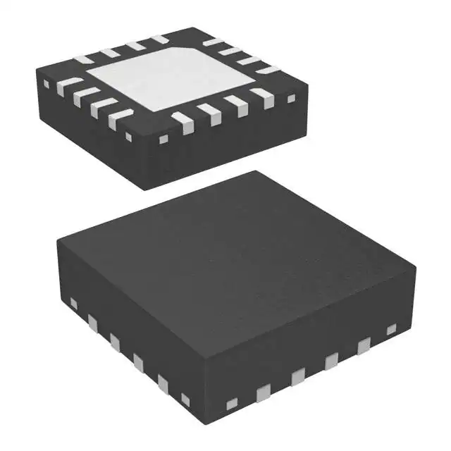
- Part No.:
- HMC1118LP3DETR
- Manufacturer:
- Analog Devices Inc.
- Package:
- 16-VFQFN Exposed Pad, CSP
- Datasheet:
- HMC1118LP3DETR.pdf
- Description:
- IC RF SWITCH SPDT 13GHZ 16LFCSP
- Quantity:
-
Original Supply
Strict supplier screening and quality control support.
-
Datasheet Support
Help engineers quickly verify product specifications.
-
BOM Sourcing
Support multi-part procurement and RFQ matching.
HMC1118LP3DETR High-Isolation SPDT RF Switch Technical Guide
Analog Devices broadband silicon SPDT nonreflective RF switch with 9kHz to 13GHz operation, internally matched 50Ω ports, high isolation, low insertion loss, positive logic control, and compact 16-lead LFCSP packaging.
Product Introduction
The HMC1118LP3DETR is a broadband, high-isolation, silicon single-pole double-throw (SPDT) RF switch manufactured by Analog Devices. It operates from 9kHz to 13GHz, supporting RF signal routing across a wide range of instrumentation, communication, and microwave applications.
The device features a nonreflective, or absorptive, switching architecture. When one RF path is selected, the unselected RF port is internally terminated to 50Ω. This helps maintain predictable RF system behavior and reduces unwanted reflections from the disconnected signal path.
The HMC1118 includes three RF ports: RFC, RF1, and RF2. The common port can be connected to either RF1 or RF2 using digital control signals. Because the RF paths are bidirectional, the device can be used for either signal selection or signal distribution.
Its typical insertion loss is 0.68dB through 8GHz, with 48dB typical isolation through 8GHz. At frequencies extending to 13GHz, typical insertion loss and isolation are approximately 1.3dB and 25dB, respectively.
The device offers a typical input 1dB compression point of 37dBm and a typical input third-order intercept point of 62dBm, making it suitable for demanding RF signal chains where linearity is important.
Under the standard datasheet test conditions, the switch operates with a positive supply of +3.3V and a negative supply of -2.5V. Analog Devices also documents a single-positive-supply configuration with VSS connected to ground, although some RF power-handling and linearity performance can be reduced.
The HMC1118LP3DETR is supplied in a 16-lead LFCSP package measuring 3mm × 3mm and is specified for operation from -40°C to +85°C. The TR suffix identifies the tape-and-reel ordering format.
Key Benefits
Broadband RF Coverage
Supports signal routing from 9kHz to 13GHz, enabling one switching architecture to serve multiple RF bands.
High Isolation
Provides 48dB typical isolation through 8GHz, helping reduce signal leakage between selected and unselected paths.
Absorptive Switching
Internally terminates the disconnected RF path into 50Ω to minimize unwanted reflections.
Compact RF Integration
Combines broadband RF switching and digital control in a 3mm × 3mm surface-mount package.
Features
- Broadband silicon SPDT RF switch
- Operating frequency range from 9kHz to 13GHz
- Nonreflective, absorptive switching architecture
- Internally matched 50Ω RF ports
- Typical insertion loss of 0.5dB through 3GHz
- Typical insertion loss of 0.68dB through 8GHz
- Typical insertion loss of 1.3dB through 13GHz
- Typical isolation of 50dB through 3GHz
- Typical isolation of 48dB through 8GHz
- Typical isolation of 25dB through 13GHz
- 37dBm typical input 1dB compression point
- 62dBm typical input third-order intercept point
- 35dBm recommended through-path RF power under specified conditions
- 27dBm recommended terminated-path RF power under specified conditions
- Positive digital control logic using 0V and 3.3V levels
- Logic-select input for configurable switching polarity
- Typical RF settling time of 7.5µs to within 0.05dB of final output
- Typical switching on/off time of 2.7µs
- Typical RF rise/fall time of 0.85µs
- Low-frequency-spurious-free switching architecture
- Bidirectional RF signal operation
- Low typical positive-supply current of 20µA
- 2kV human-body-model ESD rating
- 16-lead 3mm × 3mm LFCSP package
- Operating temperature range of -40°C to +85°C
Engineering Note: RF insertion loss, isolation, return loss, and power-handling capability vary with frequency and operating conditions. The 13GHz operating limit does not imply identical RF performance throughout the entire frequency range.
Package
The HMC1118LP3DETR uses a compact 16-lead lead-frame chip-scale package (LFCSP) with an exposed ground pad.
- Package Type: LFCSP-16
- Package Option: CP-16-38
- Nominal Body Size: 3.0mm × 3.0mm
- Nominal Package Height: 0.85mm
- Lead Pitch: 0.50mm
- Pin Count: 16
- Exposed Ground Pad: Yes
- Mounting Type: Surface Mount
- Packaging: Tape and Reel
- Moisture Sensitivity Level: MSL 3
- Maximum Reflow Temperature: 260°C
- Operating Temperature: -40°C to +85°C
- RoHS Compliance: Yes
- Product Status: PRODUCTION
The exposed pad on the bottom of the package must connect to the PCB RF and DC ground. This connection is essential for stable grounding and the intended RF performance.
The RF layout should use controlled-impedance transmission lines, a continuous ground reference, and short connections between the switch and adjacent RF components.
For production, use the official CP-16-38 mechanical drawing and recommended PCB footprint rather than a generic 16-pin QFN land pattern.
Pinout
The HMC1118LP3DETR pinout contains three RF ports, two digital control inputs, positive and negative supply connections, and multiple ground pins.
| Pin | Signal | Function |
|---|---|---|
| 1 | GND | RF and DC ground. |
| 2 | GND | RF and DC ground. |
| 3 | RFC | Common RF port, internally matched to 50Ω. |
| 4 | GND | RF and DC ground. |
| 5 | GND | RF and DC ground. |
| 6 | GND | RF and DC ground. |
| 7 | RF2 | RF port 2, internally matched to 50Ω. |
| 8 | GND | RF and DC ground. |
| 9 | VSS | Negative supply connection, nominally -2.5V. |
| 10 | VCTRL | Digital switching-control input. |
| 11 | LS | Logic-select input for control polarity. |
| 12 | VDD | Positive supply connection, nominally +3.3V. |
| 13 | GND | RF and DC ground. |
| 14 | RF1 | RF port 1, internally matched to 50Ω. |
| 15 | GND | RF and DC ground. |
| 16 | GND | RF and DC ground. |
| Exposed Pad | GND | Connect directly to PCB RF and DC ground. |
RF Port Coupling: RFC, RF1, and RF2 are DC-coupled and internally matched to 50Ω. Use DC-blocking capacitors whenever the connected RF line has a DC potential different from 0V.
Control Truth Table:
| LS | VCTRL | RFC to RF1 | RFC to RF2 |
|---|---|---|---|
| HIGH | LOW | ON | OFF |
| HIGH | HIGH | OFF | ON |
| LOW | LOW | OFF | ON |
| LOW | HIGH | ON | OFF |
In the OFF state, the unselected RF port is internally terminated to 50Ω. The control input must be driven to a valid logic level; floating control pins can produce unpredictable switching behavior.
Specifications
| Parameter | Value |
|---|---|
| Part Number | HMC1118LP3DETR |
| Manufacturer | Analog Devices |
| Device Type | SPDT RF Switch |
| Switch Architecture | Silicon, Nonreflective / Absorptive |
| Minimum Operating Frequency | 9kHz |
| Maximum Operating Frequency | 13GHz |
| RF Port Impedance | 50Ω |
| Typical Insertion Loss, to 3GHz | 0.5dB |
| Typical Insertion Loss, to 8GHz | 0.68dB |
| Typical Insertion Loss, to 13GHz | 1.3dB |
| Typical Isolation, to 3GHz | 50dB |
| Typical Isolation, to 8GHz | 48dB |
| Typical Isolation, to 13GHz | 25dB |
| Typical On-State Return Loss, to 8GHz | 22dB |
| Typical Input P1dB | 37dBm |
| Typical Input IIP3 | 62dBm |
| Recommended Through-Path Power | 35dBm under specified conditions |
| Recommended Terminated-Path Power | 27dBm under specified conditions |
| Typical RF Settling Time, 0.05dB | 7.5µs |
| Typical RF Settling Time, 0.1dB | 6µs |
| Typical Switching On/Off Time | 2.7µs |
| Typical RF Rise/Fall Time | 0.85µs |
| Positive Supply Voltage | 3.0V to 3.6V |
| Nominal Positive Supply | +3.3V |
| Negative Supply Voltage | -2.75V to -2.25V |
| Nominal Negative Supply | -2.5V |
| Single Positive Supply Operation | Supported with performance tradeoffs |
| Digital Control Low | 0.8V maximum |
| Digital Control High | 2.0V minimum |
| Typical Positive Supply Current | 20µA |
| Maximum Positive Supply Current | 200µA |
| Typical Negative Supply Current | 0.5µA |
| Maximum Negative Supply Current | 10µA |
| ESD Rating | 2kV HBM |
| Operating Temperature | -40°C to +85°C |
| Package Type | LFCSP-16 |
| Package Option | CP-16-38 |
| Package Body | 3mm × 3mm |
| Lead Pitch | 0.50mm |
| Mounting Type | Surface Mount |
| Moisture Sensitivity | MSL 3 |
| Packaging | Tape and Reel |
| Product Status | PRODUCTION |
Insertion Loss: Typical insertion loss increases with frequency. Designers should use the manufacturer's frequency-dependent curves and S-parameter files when calculating a complete RF link budget.
Isolation: The HMC1118 provides strong isolation at lower microwave frequencies. Isolation decreases toward the upper end of the operating band, so system requirements must be evaluated at the actual operating frequency.
Power Handling: Recommended through-path and terminated-path RF power ratings are different. The terminated path generally supports lower power because the disconnected RF port absorbs incident energy in its internal termination.
Single-Supply Operation: The HMC1118 can operate with VSS connected to ground. However, the RF compression point and third-order intercept performance may differ from the standard dual-supply specifications.
Control Timing: Switching time and final RF amplitude settling time are different specifications. Systems requiring accurate amplitude immediately after switching should consider the longer settling-time value.
Equivalent
When evaluating an HMC1118LP3DETR equivalent or replacement, engineers should compare frequency range, insertion loss, isolation, absorptive behavior, power handling, control logic, supply requirements, package dimensions, and RF pin arrangement.
HMC1118LP3DE: The same HMC1118 device supplied in a non-tape-and-reel ordering format. It uses the same 16-lead CP-16-38 LFCSP package and is the closest alternative when only the shipping configuration differs.
HMC1118 Family: The original HMC1118 family remains the preferred choice for existing designs requiring its specific control logic, broadband RF characteristics, and 3mm × 3mm package.
ADRF5020: A related Analog Devices broadband SPDT RF switch that may be considered for applications requiring higher-frequency coverage. Its control interface, RF performance, and package must be evaluated separately.
ADRF5024: Another Analog Devices RF switch option for broadband routing applications. It is not a guaranteed pin-compatible substitute for the HMC1118.
Other Absorptive SPDT Switches: Alternative RF switches may offer similar frequency coverage or isolation, but their RF terminations, power-handling limits, and control timing can differ significantly.
Replacement Recommendation: For an existing HMC1118LP3DETR design, the HMC1118LP3DE is the most direct ordering alternative. Cross-family replacements require RF simulation, PCB review, control-logic verification, and performance testing.
Manufacturer
Analog Devices, Inc. is a global semiconductor manufacturer specializing in analog, mixed-signal, RF, microwave, and power-management technologies.
The HMC1118 is part of the company's RF and microwave switch portfolio, incorporating technology associated with the former Hittite Microwave product family.
The HMC1118LP3DETR is identified by Analog Devices as a PRODUCTION product and is supplied in a 16-lead LFCSP package.
Official Product Page: Analog Devices HMC1118
Official Datasheet: HMC1118 Datasheet, Revision A
Manufacturer Website: www.analog.com
For procurement, verify the full ordering number, package marking, original tape-and-reel packaging, moisture sensitivity, manufacturing traceability, and current product status.
Applications
RF Test Instrumentation
Switches RF signals between measurement paths, test ports, calibration networks, and receiver inputs.
Microwave Radio and VSAT
Supports RF signal selection and routing in microwave communication and satellite terminal systems.
Military RF Equipment
Provides broadband signal routing in suitable military radio and electronic countermeasure applications.
Radar Systems
Routes RF signals between compatible radar receiver, test, and signal-processing paths.
Broadband Telecommunications
Supports RF path selection in broadband communication and fiber-optic infrastructure equipment.
RF Signal Distribution
Enables bidirectional selection between two RF signal paths while terminating the unselected port.
Typical Application Circuit: Connect the common RF signal to RFC and the selectable RF paths to RF1 and RF2. Use controlled-impedance 50Ω PCB transmission lines and suitable RF connectors.
Connect VDD to the positive supply and VSS to the negative supply for standard dual-supply operation. Place suitable bypass capacitors close to the supply pins.
Drive VCTRL and LS using compatible digital logic. The LS input determines whether a high or low VCTRL signal selects the RFC-to-RF1 path.
Absorptive Switching: When one RF port is disconnected, the device internally terminates that port into 50Ω. This behavior helps reduce reflections in sensitive RF networks.
Bidirectional Operation: The RF paths are bidirectional. Depending on the system architecture, the switch can select one of two sources or direct one signal toward one of two destinations.
RF Layout: Maintain 50Ω impedance at all RF ports, minimize trace discontinuities, and connect the ground pins and exposed pad directly to the RF ground plane.
DC Blocking: Because the RF ports are DC-coupled, use external blocking capacitors when the RF line potential differs from 0V. Capacitor selection must account for the required low-frequency cutoff and RF performance.
Power-Up Sequence: Establish ground first, then apply VDD and VSS, followed by the digital control inputs and RF signal. Driving control pins before the supply can forward-bias internal protection structures.
Single-Supply Configuration: For systems without a negative supply, VSS may be tied to ground according to the manufacturer's documented application guidance. The resulting RF performance must be verified against the application requirements.
Evaluation and Validation: Analog Devices provides the EV1HMC1118LP3D evaluation board and S-parameter resources. These are useful for validating insertion loss, isolation, matching, and RF behavior before final PCB release.
Disclaimer
This technical guide is provided for product identification, engineering reference, and procurement support. All electrical specifications, RF performance limits, supply requirements, control logic, pin assignments, power-handling ratings, package dimensions, moisture sensitivity, environmental ratings, and lifecycle information should be verified against the latest Analog Devices documentation before design or purchase. Typical RF characteristics are not guaranteed across all frequencies, temperatures, supply conditions, and PCB layouts. Single-supply operation may change compression and linearity performance. Suggested alternatives are not guaranteed direct replacements. RF system qualification, electromagnetic compatibility, power derating, and layout validation remain the responsibility of the equipment designer. Pricing and availability may change without notice.