


MAX3232ESE+ Analog Devices | RS-232 Transceiver Technical Guide
Product Technical Guide MAX3232ESE+ Dual RS-232 Transceiver Technical GuideAnalog Devices / Maxim Integrated dual-driver, dual-receiver RS-232 transceiver featuring 3.0V to 5.5V single-supply operation…
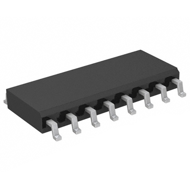
- Part No.:
- MAX3232ESE+
- Manufacturer:
- Analog Devices Inc./Maxim Integrated
- Package:
- 16-SOIC (0.154", 3.90mm Width)
- Datasheet:
- MAX3232ESE+.pdf
- Description:
- IC TXRX 16-SOIC
- Quantity:
-
Original Supply
Strict supplier screening and quality control support.
-
Datasheet Support
Help engineers quickly verify product specifications.
-
BOM Sourcing
Support multi-part procurement and RFQ matching.
MAX3232ESE+ Analog Devices | RS-232 Transceiver Technical Guide
Analog Devices / Maxim Integrated dual-driver, dual-receiver RS-232 transceiver featuring 3.0V to 5.5V single-supply operation, integrated charge pumps, up to 235kbps data rate, and 16-pin narrow SOIC packaging.
Product Introduction
The MAX3232ESE+ is a dual-driver, dual-receiver RS-232 interface transceiver originally developed by Maxim Integrated, now part of Analog Devices. It provides the electrical conversion required to connect low-voltage TTL/CMOS digital logic with equipment using conventional RS-232 signaling.
The device integrates two RS-232 transmitters and two RS-232 receivers, allowing two independent signal channels to operate in both directions. This configuration supports full-duplex serial communication and hardware-handshaking arrangements when used with an appropriate controller and connector configuration.
Unlike traditional RS-232 interface devices that require separate positive and negative power supplies, the MAX3232ESE+ operates from a single 3.0V to 5.5V supply. Its internal dual charge-pump circuitry generates the positive and negative voltages needed for compliant RS-232 output signaling.
The charge-pump architecture uses four external capacitors, typically 0.1µF each, while a separate supply bypass capacitor is recommended for stable operation.
The MAX3232ESE+ supports a specified maximum data rate of 235kbps, making it suitable for industrial serial interfaces, microcontroller communication, diagnostic connections, and legacy equipment integration.
The device is supplied in a 16-pin narrow SOIC package and supports an operating temperature range of -40°C to +85°C.
Its integrated voltage conversion, low supply current, and established RS-232 interface architecture make it a practical choice for embedded systems requiring reliable asynchronous serial communication.
Key Benefits
Dual-Channel Communication
Two transmitters and two receivers support full-duplex RS-232 communication and additional serial control signals.
Single-Supply Operation
Operates from 3.0V to 5.5V without requiring external positive and negative RS-232 power rails.
Integrated Charge Pumps
Internal voltage conversion uses four small external capacitors to generate the required RS-232 signaling voltages.
Compact SOIC Package
The 16-pin surface-mount package supports established PCB layouts and automated assembly processes.
Features
- Dual-driver, dual-receiver RS-232 transceiver
- Two RS-232 transmitter channels
- Two RS-232 receiver channels
- Full-duplex communication capability
- Single 3.0V to 5.5V supply operation
- Integrated positive and negative charge-pump converters
- Four external 0.1µF charge-pump capacitors for typical operation
- TTL/CMOS-compatible transmitter inputs
- TTL/CMOS-compatible receiver outputs
- RS-232-compatible transmitter output voltage levels
- Maximum specified data rate of 235kbps
- Typical receiver hysteresis of approximately 0.3V
- Low supply current, approximately 0.3mA under specified conditions
- RS-232 receiver inputs tolerant of specified high positive and negative voltages
- 16-pin narrow SOIC surface-mount package
- Operating temperature range from -40°C to +85°C
- Lead-free ordering designation indicated by the + suffix
- Available in tube and tape-and-reel ordering options
Design Note: The MAX3232ESE+ performs RS-232 electrical-level conversion. It does not convert RS-232 into USB, RS-485, CAN, or Ethernet protocols. The connected controller must provide the appropriate UART or asynchronous serial communication logic.
Package
The MAX3232ESE+ uses a 16-pin narrow SOIC surface-mount package suitable for conventional printed circuit board assembly.
- Package Type: SOIC
- Package Configuration: Narrow SOIC
- Package Code: ESE
- Pin Count: 16
- Nominal Body Width: 3.9mm
- Nominal Body Length: Approximately 9.9mm
- Lead Pitch: 1.27mm
- Mounting Type: Surface Mount
- Standard MAX3232ESE+ Packaging: Tube
- Tape-and-Reel Ordering Option: MAX3232ESE+T
- Operating Temperature Grade: -40°C to +85°C
- Lead-Free Ordering Designation: + suffix
The narrow SOIC package provides sufficient lead spacing for standard automated assembly and simplifies inspection compared with smaller leadless package alternatives.
For reliable charge-pump operation, the external capacitors should be placed close to their corresponding device pins. A local supply bypass capacitor should also be located near VCC and GND.
PCB designers should follow the manufacturer's latest mechanical drawing and recommended land pattern for the specific ordering number.
Pinout
The MAX3232ESE+ pinout consists of two transmitter inputs, two transmitter outputs, two receiver inputs, two receiver outputs, charge-pump connections, and power supply terminals.
| Pin | Signal | Function |
|---|---|---|
| 1 | C1+ | Positive terminal of the charge-pump voltage-doubler capacitor. |
| 2 | V+ | Positive voltage generated by the internal charge pump. |
| 3 | C1- | Negative terminal of the voltage-doubler capacitor. |
| 4 | C2+ | Positive terminal of the charge-pump inverter capacitor. |
| 5 | C2- | Negative terminal of the charge-pump inverter capacitor. |
| 6 | V- | Negative voltage generated by the internal charge pump. |
| 7 | T2OUT | RS-232-level output from transmitter channel 2. |
| 8 | R2IN | RS-232-level input to receiver channel 2. |
| 9 | R2OUT | TTL/CMOS-level output from receiver channel 2. |
| 10 | T2IN | TTL/CMOS-level input to transmitter channel 2. |
| 11 | T1IN | TTL/CMOS-level input to transmitter channel 1. |
| 12 | R1OUT | TTL/CMOS-level output from receiver channel 1. |
| 13 | R1IN | RS-232-level input to receiver channel 1. |
| 14 | T1OUT | RS-232-level output from transmitter channel 1. |
| 15 | GND | Ground reference. |
| 16 | VCC | Positive power supply input, 3.0V to 5.5V. |
Important: The pin assignments above apply to the MAX3232ESE+ 16-pin SOIC package. Verify package orientation, pin numbering, and capacitor connections against the latest Analog Devices documentation before PCB fabrication.
Unused transmitter inputs should be tied to a defined logic level rather than left floating. The generated V+ and V- nodes are intended for charge-pump operation and should not be treated as general-purpose auxiliary power supplies.
Specifications
| Parameter | Value |
|---|---|
| Part Number | MAX3232ESE+ |
| Manufacturer | Analog Devices / Maxim Integrated |
| Product Family | MAX3232 |
| Device Type | RS-232 Driver / Receiver Transceiver |
| Interface Standard | RS-232 |
| Number of Drivers | 2 |
| Number of Receivers | 2 |
| Communication Duplex | Full Duplex |
| Supply Voltage Range | 3.0V to 5.5V |
| Maximum Data Rate | 235kbps |
| Receiver Hysteresis | 0.3V typical |
| Typical Supply Current | 0.3mA under specified conditions |
| Charge-Pump Architecture | Integrated Dual Charge Pump |
| External Charge-Pump Capacitors | Four, typically 0.1µF each |
| Recommended Supply Bypass Capacitor | 0.1µF, subject to circuit requirements |
| Logic Interface | TTL / CMOS |
| Receiver Input Voltage Range | Up to ±25V under specified limits |
| Driver Output Level | RS-232 compatible |
| Receiver Propagation Delay | Approximately 0.3µs typical |
| Maximum Driver Slew Rate | 30V/µs under specified load conditions |
| Operating Temperature Range | -40°C to +85°C |
| Package Type | Narrow SOIC |
| Package Code | ESE |
| Pin Count | 16 |
| Mounting Type | Surface Mount |
| Packaging | Tube |
| Tape-and-Reel Option | MAX3232ESE+T |
| Lead-Free Version | Yes, + suffix |
| Product Status | Active, subject to manufacturer confirmation |
RS-232 Level Conversion: The transmitter converts logic-level input signals into positive and negative RS-232 voltage levels. The receiver converts RS-232 input signals into logic-level outputs suitable for the host controller.
Charge-Pump Operation: The internal converters generate the positive and negative voltage rails required for RS-232 communication. Four external charge-pump capacitors are used in the typical application circuit.
Data Rate: The maximum specified data rate is 235kbps. Actual communication performance depends on cable length, load capacitance, supply voltage, noise environment, and the connected serial equipment.
Logic Compatibility: Receiver outputs are referenced to the device supply voltage. Designers must ensure the output levels are compatible with the connected MCU or processor, particularly when using different logic supply domains.
Power Supply Decoupling: A local bypass capacitor should be placed between VCC and GND. Charge-pump capacitors should be selected and placed according to the manufacturer's recommended circuit.
Protection Consideration: The transceiver's electrical limits do not eliminate the need for system-level ESD and surge protection. Externally accessible RS-232 ports may require additional protection depending on the installation environment.
Equivalent
When evaluating a MAX3232ESE+ equivalent, replacement, or alternative, compare supply voltage, number of transmitters and receivers, RS-232 output performance, data rate, capacitor requirements, pin configuration, package dimensions, and operating temperature range.
MAX3232ESE+T: The same Analog Devices / Maxim Integrated device supplied in tape-and-reel packaging. This is a practical procurement alternative where automated assembly requires reel packaging.
MAX3232CSE+: A related MAX3232 ordering variant in a 16-pin SOIC package. Temperature grade and ordering specifications differ, so suitability must be checked before substitution.
MAX3232EUE+: A related MAX3232 device supplied in a 16-pin TSSOP package. Its package footprint differs from the ESE SOIC version, making it unsuitable as a direct mechanical replacement.
Texas Instruments MAX3232: A functionally similar dual-driver, dual-receiver RS-232 transceiver family. Specific ordering numbers and package options must be checked for electrical and pin compatibility.
Texas Instruments TRS3232E: A related RS-232 interface family offering enhanced ESD characteristics in certain variants. Verify supply voltage, data rate, pinout, capacitor requirements, and package before considering replacement.
SP3232E Series: A comparable dual-channel RS-232 transceiver family offered under legacy Sipex/Exar product lines. The selected manufacturer and ordering variant must be verified for availability and compatibility.
Replacement Recommendation: For existing MAX3232ESE+ PCB assemblies, prioritize the original device or the MAX3232ESE+T packaging variant. For cross-manufacturer substitutions, validate charge-pump capacitor values, pin assignments, output drive characteristics, ESD performance, and operating temperature before production approval.
Manufacturer
Analog Devices, Inc. (ADI) is a semiconductor manufacturer specializing in analog, mixed-signal, power management, interface, sensing, and signal-processing technologies.
The MAX3232 family originated from Maxim Integrated, which became part of Analog Devices in 2021. The product continues to be identified through its established Maxim ordering number.
The MAX3232 family is used in embedded and industrial electronic systems that require communication between modern low-voltage controllers and conventional RS-232 serial equipment.
Official Product Family: MAX3232 – Analog Devices
Official Datasheet: MAX3222–MAX3241 RS-232 Transceiver Family Datasheet
Manufacturer Website: www.analog.com
For procurement, confirm the complete ordering number, original manufacturer, packaging format, date code, lot traceability, and applicable environmental documentation.
Applications
Industrial Control Systems
RS-232 communication between industrial controllers, programmable logic controllers, monitoring systems, and serial peripheral equipment.
Microcontroller Interfaces
Conversion between MCU UART logic levels and external RS-232 serial communication ports.
Serial Communication Equipment
Bidirectional RS-232 interface conversion for embedded communication modules and legacy serial devices.
Diagnostic and Service Ports
Serial maintenance, equipment configuration, debugging, and diagnostic connections.
Networking Equipment
RS-232 console and management interfaces for compatible routers, switches, and communication hardware.
Embedded Electronic Systems
Communication between embedded processors and instruments, terminals, or other equipment using RS-232 electrical signaling.
Application Note: In a typical MCU-to-RS-232 interface, the controller's UART TX signal connects to T1IN, and T1OUT connects to the receiving RS-232 input of the external device. The external RS-232 transmit signal connects to R1IN, while R1OUT connects to the controller's UART RX input.
The second transmitter and receiver may be used for another communication channel or compatible hardware-handshaking signals.
For standard operation, install the required charge-pump capacitors and a local VCC bypass capacitor. Verify signal-ground continuity, connector wiring, cable characteristics, and external ESD protection requirements.
Interface Warning: RS-232 voltage levels are not directly compatible with ordinary MCU GPIO pins. Do not connect external RS-232 signals directly to a microcontroller UART without suitable interface circuitry.
Disclaimer
This technical guide is provided for general product identification, engineering reference, and procurement support. All electrical specifications, data rates, supply voltage limits, capacitor requirements, pin assignments, package dimensions, environmental compliance information, and product lifecycle status should be verified against the latest Analog Devices documentation before design or purchase. Suggested alternatives are not guaranteed direct replacements. Application performance depends on the complete circuit design, cable loading, power supply conditions, and operating environment. Product prices and availability may change without notice.