


TPS61022RWUR Texas Instruments | 8A Boost Converter Datasheet, Pinout & Equivalent
Product Technical Guide TPS61022RWUR 8A Synchronous Boost Converter Technical GuideTexas Instruments TPS61022RWUR is a high-efficiency synchronous step-up DC/DC converter featuring a 0.5V to 5.5V opera…
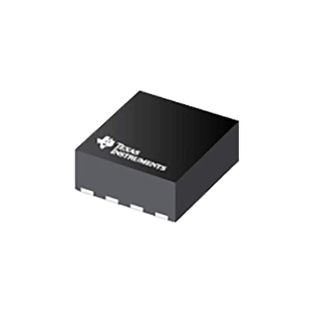
- Part No.:
- TPS61022RWUR
- Manufacturer:
- Texas Instruments
- Package:
- 7-VFQFN
- Datasheet:
- TPS61022RWUR.pdf
- Description:
- IC REG BOOST ADJ 8A 7VQFN
- Quantity:
-
Original Supply
Strict supplier screening and quality control support.
-
Datasheet Support
Help engineers quickly verify product specifications.
-
BOM Sourcing
Support multi-part procurement and RFQ matching.
TPS61022RWUR Texas Instruments | 8A Boost Converter Datasheet, Pinout & Equivalent
Texas Instruments TPS61022RWUR is a high-efficiency synchronous step-up DC/DC converter featuring a 0.5V to 5.5V operating input range, adjustable 2.2V to 5.5V output, 8A typical valley switch current limit, and a compact 7-pin VQFN-HR package.
Product Introduction
The TPS61022RWUR is a high-efficiency synchronous boost converter manufactured by Texas Instruments. It is designed to generate a regulated higher output voltage from low-voltage sources, including single-cell lithium-ion batteries, primary batteries, and supercapacitors.
The converter supports an operating input voltage range of 0.5V to 5.5V and an adjustable output voltage range of 2.2V to 5.5V. A minimum input voltage of approximately 1.8V is required for initial startup. Once the device starts and the output voltage exceeds the required threshold, operation can continue with input voltages as low as 0.5V.
Unlike a basic asynchronous boost regulator, the TPS61022 integrates both low-side and high-side power MOSFETs. Its synchronous architecture reduces rectification losses and helps achieve high conversion efficiency.
Texas Instruments specifies a typical efficiency of 94.7% when converting 3.6V to 5V at a 3A output load under the stated test conditions.
The device features an 8A typical valley switch current limit, with a minimum guaranteed valley current limit of 6.5A across the specified temperature range. This rating describes internal switch current capability rather than a fixed output-current rating.
The TPS61022 also provides selectable automatic pulse-frequency modulation (PFM) and forced pulse-width modulation (PWM), allowing designers to prioritize light-load efficiency or switching-frequency behavior.
The device is available in a compact 2mm × 2mm, 7-pin VQFN-HR package, suitable for portable electronics, embedded systems, and space-constrained power-management designs.
Key Benefits
Ultra-Low Input Operation
Operates from input voltages down to 0.5V after startup, supporting deeply discharged supercapacitors and low-voltage battery sources.
High Conversion Efficiency
Integrated synchronous MOSFETs enable 94.7% efficiency at a specified 3.6V-to-5V, 3A operating point.
Compact Power Solution
2mm × 2mm VQFN-HR package and integrated compensation help minimize external component count.
Integrated Protection
Includes undervoltage lockout, output overvoltage protection, short-circuit protection, and thermal shutdown.
Features
- High-efficiency synchronous boost DC/DC converter
- 0.5V to 5.5V operating input voltage range
- 1.8V minimum input voltage required for startup
- 2.2V to 5.5V adjustable output voltage range
- 8A typical valley switch current limit
- 6.5A minimum valley switch current limit over the specified temperature range
- 94.7% efficiency at VIN = 3.6V, VOUT = 5V, and IOUT = 3A
- Integrated 12mΩ low-side power MOSFET
- Integrated 18mΩ high-side power MOSFET
- Approximately 1MHz switching frequency when VIN exceeds 1.5V
- Approximately 600kHz switching frequency when VIN is below 1V
- Automatic PFM or forced PWM operation selectable through MODE
- Approximately 26µA typical quiescent current from VOUT in light-load operation
- Internal loop compensation
- Input-to-output pass-through operation when VIN exceeds VOUT
- True input-to-output load disconnection during shutdown
- Soft-start and undervoltage-lockout functions
- Output overvoltage and short-circuit protection
- Thermal shutdown protection
- Operating junction temperature range of -40°C to +125°C
- Compact 7-pin VQFN-HR package
Design Note: The maximum deliverable output current is dependent on the input voltage, output voltage, inductor characteristics, conversion efficiency, and thermal conditions. The 8A switch-current specification must not be interpreted as an 8A continuous output-current rating.
Package
The TPS61022RWUR is supplied in Texas Instruments' RWU VQFN-HR package.
- Package Code: RWU
- Package Type: VQFN-HR
- Terminal Count: 7
- Nominal Body Length: 2.00mm
- Nominal Body Width: 2.00mm
- Package Area: 4mm²
- Thermal Pad: Present
- Mounting: Surface Mount
- Ordering Part Number: TPS61022RWUR
- Packaging: Tape and Reel
The package is optimized for compact power-conversion applications. Its exposed thermal pad and PCB copper layout are important for heat dissipation and electrical performance.
Use the official TI RWU package drawing to verify land-pattern dimensions, pad placement, pin orientation, and assembly requirements.
Place the power inductor and input/output ceramic capacitors close to the converter to minimize parasitic resistance and switching-loop inductance.
Pinout
The TPS61022RWUR has seven functional pins and a thermal pad. The following assignments correspond to the official Texas Instruments RWU package pin-function table.
| Pin | Symbol | Function |
|---|---|---|
| 1 | GND | Ground connection. Connect the output capacitor ground close to this terminal. |
| 2 | SW | Switching node connected to the integrated power MOSFETs and external inductor. |
| 3 | VOUT | Boost converter output connection. |
| 4 | FB | Feedback input used to set the regulated output voltage. |
| 5 | EN | Enable input. Logic high enables operation; logic low initiates shutdown. |
| 6 | MODE | Light-load operating-mode selection. High selects forced PWM; low selects automatic PFM. |
| 7 | VIN | Input power-supply connection. |
Typical Connection: Connect an appropriate power inductor between VIN and SW. Connect the input capacitor between VIN and GND and the output capacitors between VOUT and GND.
Connect a resistor divider between VOUT and GND, with its midpoint connected to FB. Select the resistor values according to the output-voltage-setting equation in the official datasheet.
Connect EN to a valid logic control signal. Configure MODE according to the application's light-load efficiency and output-ripple requirements.
Important: The device has seven functional pins, not nine. Always verify the physical pin orientation and thermal-pad connection using the official package drawing.
Specifications
| Parameter | Value |
|---|---|
| Part Number | TPS61022RWUR |
| Manufacturer | Texas Instruments |
| Product Family | TPS61022 |
| Device Category | DC/DC Switching Regulator |
| Topology | Synchronous Boost |
| Number of Outputs | 1 |
| Minimum Operating Input Voltage | 0.5V after startup |
| Maximum Operating Input Voltage | 5.5V |
| Minimum Startup Input Voltage | 1.8V |
| Minimum Adjustable Output Voltage | 2.2V |
| Maximum Adjustable Output Voltage | 5.5V |
| Typical Valley Switch Current Limit | 8A |
| Minimum Valley Switch Current Limit | 6.5A |
| Typical Conversion Efficiency | 94.7% at VIN = 3.6V, VOUT = 5V, IOUT = 3A |
| Low-Side MOSFET On-Resistance | 12mΩ |
| High-Side MOSFET On-Resistance | 18mΩ |
| Switching Frequency Above 1.5V Input | Approximately 1MHz |
| Switching Frequency Below 1V Input | Approximately 600kHz |
| Typical Light-Load Quiescent Current | 26µA from VOUT |
| Operating Modes | Automatic PFM / Forced PWM |
| Output Voltage Reference Accuracy | ±2.5% over the specified temperature range |
| Maximum Duty Cycle | 97% |
| Input-to-Output Load Disconnect | Supported during shutdown |
| Pass-Through Mode | Supported |
| Output Overvoltage Protection | Integrated |
| Short-Circuit Protection | Integrated |
| Thermal Shutdown | Integrated |
| Operating Junction Temperature | -40°C to +125°C |
| Package | VQFN-HR (RWU) |
| Package Dimensions | 2mm × 2mm |
| Functional Pin Count | 7 |
| Mounting | Surface Mount |
| Packaging | Tape and Reel |
Startup Requirements: The 0.5V minimum operating input is available only after successful startup. The input voltage must initially meet the device's startup threshold.
Output Current: The converter can support substantial output power, but maximum output current varies with input voltage, output voltage, inductor selection, current-limit tolerance, efficiency, and thermal conditions.
Reference Application: TI provides a design example generating 5V at 3A from a single-cell lithium-ion battery operating between 2.7V and 4.35V.
Switching Frequency: The switching frequency changes with low input voltage. This behavior helps improve conversion efficiency and maintain operation at higher step-up ratios.
Efficiency: The 94.7% efficiency figure applies to a specific test condition and is not guaranteed across all input voltages, output voltages, and load currents.
Thermal Design: High output current increases power loss in the MOSFETs, inductor, and PCB conductors. Thermal evaluation is required for continuous operation.
Equivalent
When searching for a TPS61022RWUR equivalent or replacement, compare the input voltage range, startup voltage, output-voltage range, switch current limit, efficiency, control mode, switching frequency, protection features, package, and pinout.
TPS61022RWUT: A related Texas Instruments ordering variant of the TPS61022 in the RWU package, supplied in a different tape-and-reel quantity. Verify ordering and packaging requirements before substitution.
TPS61023: A related Texas Instruments boost converter suitable for evaluation in applications requiring similar low-voltage step-up functionality. Its electrical ratings, switching behavior, and package connections must be compared before use.
TPS61021A: Another TI synchronous boost converter family that may be considered for low-voltage battery-powered systems. It is not automatically a pin-compatible replacement.
TPS61236P: A TI boost-converter option for certain higher-power battery applications. Input range, output current capability, and PCB requirements differ from the TPS61022.
Alternative Boost Converters: Other manufacturers offer synchronous step-up regulators for portable and battery-powered devices. Their suitability depends on the complete system requirements.
Replacement Recommendation: For an existing PCB, first evaluate another verified TPS61022 RWU ordering variant. Substituting a different boost-converter family normally requires electrical validation and may require PCB redesign.
Manufacturer
Texas Instruments Incorporated is a semiconductor manufacturer specializing in analog integrated circuits, embedded processing, power management, and signal-chain technologies.
The TPS61022 belongs to TI's synchronous boost-converter portfolio, targeting efficient voltage conversion from low-voltage energy sources.
Official Product Page: Texas Instruments TPS61022
Official Datasheet: TPS61022 8A Boost Converter Datasheet
Manufacturer Website: www.ti.com
Distributor Reference: TPS61022RWUR Product Listing
When purchasing, verify the complete ordering code, original manufacturer packaging, device marking, lot traceability, and product lifecycle status.
Applications
Battery-Powered Electronics
Generates regulated supply rails from single-cell battery sources.
Portable Devices
Supports compact equipment requiring efficient 3.3V or 5V power conversion.
Supercapacitor Backup Power
Maintains regulated output during supported supercapacitor discharge conditions.
IoT Devices
Provides efficient voltage boosting for connected sensors and communication modules.
Wireless Communication Modules
Supports compatible communication systems with pulsed load-current requirements.
USB Power Supplies
Generates regulated 5V rails from suitable lower-voltage sources.
Typical Lithium-Ion Battery Application: TI demonstrates the TPS61022 operating from a 2.7V to 4.35V lithium-ion battery and generating a regulated 5V output at up to 3A under the example design conditions.
The reference circuit uses a 1µH power inductor, a 10µF input capacitor, and three 22µF output capacitors. The feedback divider uses 732kΩ and 100kΩ resistors to establish the required output voltage.
Battery Voltage Conversion: As battery voltage decreases, the converter increases its boost ratio to maintain the output. The required input current generally rises as the input voltage falls for a constant output-power demand.
Supercapacitor Backup: The converter's ability to continue operating from a 0.5V input after startup is useful in energy-storage systems that allow deep supercapacitor discharge. The available output power at very low input voltage is limited by current and efficiency constraints.
PFM vs PWM Selection: Automatic PFM mode can improve light-load efficiency, making it attractive for systems with long standby periods. Forced PWM may be preferable where more predictable switching-frequency behavior is important.
Inductor Selection: Choose an inductor with suitable inductance, saturation-current rating, DC resistance, and thermal characteristics. The inductor must withstand the peak current encountered under the worst-case input and load conditions.
Capacitor Selection: Ceramic capacitor effective capacitance decreases under DC bias. Verify that the selected input and output capacitors provide adequate effective capacitance at their actual operating voltages.
PCB Layout: Minimize the high-current switching-loop area. Position the input capacitor, inductor, and output capacitors close to the converter. Route the FB signal away from noisy switching traces.
System Validation: Evaluate startup at the lowest expected input voltage, full-load regulation, transient response, short-circuit behavior, output ripple, inductor temperature, and converter junction temperature.
Disclaimer
This technical guide is provided for product identification, engineering reference, and procurement support. All electrical specifications, pin assignments, package dimensions, efficiency values, current limits, protection thresholds, and application requirements must be verified against the latest official Texas Instruments datasheet before design or purchase. The TPS61022RWUR has an 8A typical valley switch current limit, not an unconditional 8A output-current rating. Operation from a 0.5V input requires successful startup at the specified higher startup voltage. Suggested alternatives are not guaranteed direct replacements. Product availability, lifecycle status, pricing, and lead times may change without notice.