


XC7Z010-1CLG400I AMD Xilinx Zynq-7000 SoC FPGA – Datasheet, Pinout, Specifications & Applications
Product Technical Guide XC7Z010-1CLG400I Zynq-7000 SoC FPGA Technical GuideExplore the AMD Xilinx XC7Z010-1CLG400I, featuring a dual-core Arm Cortex-A9 processing system, 28K programmable logic cells, …
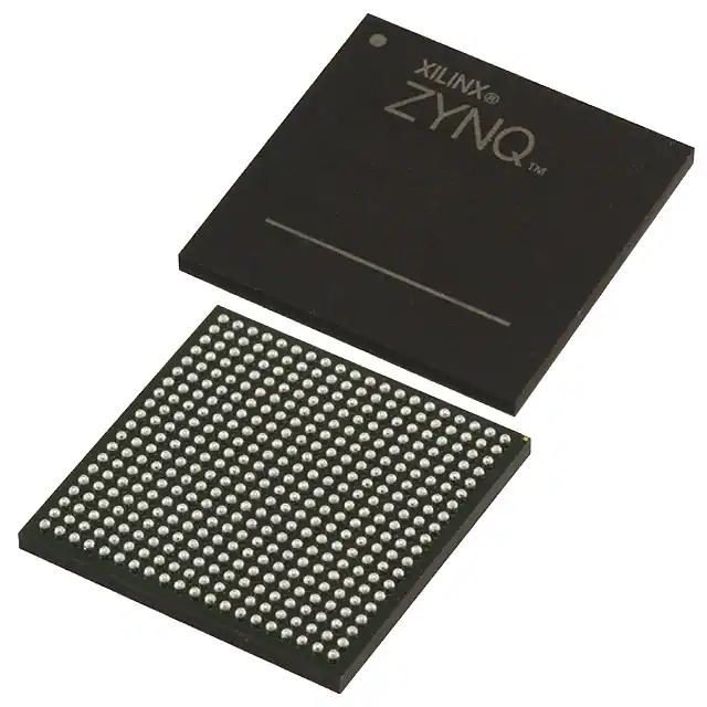
- Part No.:
- XC7Z010-1CLG400I
- Manufacturer:
- AMD
- Package:
- 400-LFBGA, CSPBGA
- Datasheet:
- XC7Z010-1CLG400I.pdf
- Description:
- IC SOC CORTEX-A9 667MHZ 400BGA
- Quantity:
-
Original Supply
Strict supplier screening and quality control support.
-
Datasheet Support
Help engineers quickly verify product specifications.
-
BOM Sourcing
Support multi-part procurement and RFQ matching.
XC7Z010-1CLG400I AMD Xilinx Zynq-7000 SoC FPGA – Datasheet, Pinout, Specifications & Applications
Explore the AMD Xilinx XC7Z010-1CLG400I, featuring a dual-core Arm Cortex-A9 processing system, 28K programmable logic cells, 80 DSP slices, 2.1Mb block RAM, industrial temperature support, and a 400-ball CLG400 package.
Product Introduction
The XC7Z010-1CLG400I is an industrial-grade system-on-chip FPGA from the AMD Xilinx Zynq-7000 family. It combines an Arm-based processing system with programmable logic on a single semiconductor device.
The integrated processing system incorporates two 32-bit Arm Cortex-A9 processor cores, while the programmable logic uses an architecture related to the Xilinx Artix-7 FPGA family.
This combination allows developers to implement software-based control functions and customized digital hardware within one device. The processor subsystem can handle operating systems, communications, and supervisory tasks, while the FPGA fabric supports parallel processing, hardware acceleration, and application-specific interfaces.
The XC7Z010 provides 28,000 programmable logic cells, 17,600 lookup tables, 35,200 flip-flops, 80 DSP slices, and 2.1Mb of programmable-logic block RAM.
The -1 speed-grade industrial device supports processor operation up to 667MHz under the applicable clock-configuration conditions.
The CLG400 package is a 400-ball chip-scale BGA with a nominal 17mm × 17mm body and 0.8mm ball pitch.
Typical design areas include industrial automation, embedded vision, instrumentation, communications equipment, and embedded processing platforms.
Key Benefits
Processor and FPGA Integration
Combines dual Arm Cortex-A9 processors with programmable logic to support software control and hardware acceleration.
Parallel Processing Resources
Provides 28K logic cells and 80 DSP slices for configurable data processing, filtering, and digital control.
Flexible Connectivity
Integrates processing-system peripherals and configurable programmable-logic interfaces for embedded system development.
Industrial Temperature Grade
Supports a specified junction-temperature range of -40°C to +100°C for industrial-grade operation.
Features
- AMD Xilinx Zynq-7000 Z-7010 SoC architecture
- Dual-core 32-bit Arm Cortex-A9 MPCore processing system
- Processor frequency up to 667MHz under specified clock conditions
- Artix-7-class programmable logic architecture
- 28,000 programmable logic cells
- 17,600 programmable-logic lookup tables
- 35,200 programmable-logic flip-flops
- 80 DSP48E1 processing slices
- 2.1Mb programmable-logic block RAM
- 256KB on-chip memory in the processing system
- 32KB instruction and 32KB data L1 cache per processor core
- 512KB shared L2 cache
- Integrated external DDR memory controller
- High-performance AXI interfaces between processing system and programmable logic
- Integrated USB, Ethernet, SPI, I2C, UART, CAN, and SD/SDIO controllers
- Configurable processing-system MIO and programmable-logic I/O
- 100 programmable-logic HR I/O pins in the CLG400 package
- Integrated clock-management and system-monitoring functions
- JTAG debugging and programmable-logic configuration support
- Industrial temperature grade
- 400-ball CLG400 chip-scale BGA package
Package
Package Designation: CLG400
Package Type: Chip-Scale Ball Grid Array (CSBGA)
Number of Balls: 400
Nominal Body Size: 17mm × 17mm
Ball Pitch: 0.8mm
Mounting Type: Surface Mount
Speed Grade: -1
Temperature Grade: Industrial
Ordering Suffix: I
The CLG400 package provides a compact footprint for integrating a processor-based programmable system into industrial and embedded equipment.
The 400 package balls include power, ground, dedicated processing-system signals, configuration connections, and programmable-logic I/O. The total ball count must not be interpreted as the number of available user I/O pins.
PCB designers should use the official AMD package drawings and device-specific pin files when preparing the footprint, assigning I/O banks, and routing high-speed signals.
BGA assembly requires an appropriate soldering process, PCB design rules, and inspection strategy.
Pinout
The XC7Z010-1CLG400I uses a 400-ball package with separate connections for the processing system, programmable logic, power supplies, clocks, configuration, and external interfaces.
Processing System: The integrated Arm subsystem provides dedicated interfaces for memory access, boot configuration, and common embedded communications.
Programmable Logic: The FPGA fabric supports configurable digital functions, application-specific interfaces, and custom hardware acceleration.
Important Design Note: The XC7Z010 CLG400 package provides 100 programmable-logic HR I/O pins. Actual usable connections depend on bank allocation, selected I/O standards, dedicated functions, and board-level design.
Pinout Reference: Use AMD UG865, Zynq-7000 SoC Packaging and Pinout, together with the exact XC7Z010 CLG400 package pin file. Do not substitute a generic Zynq-7000 pinout or assume pin compatibility with another device.
Specifications
| Parameter | Value |
|---|---|
| Part Number | XC7Z010-1CLG400I |
| Manufacturer | AMD (formerly Xilinx) |
| Product Family | Zynq-7000 |
| Device | Z-7010 |
| Device Type | System-on-Chip FPGA |
| Processing Architecture | Dual-core Arm Cortex-A9 |
| Processor Word Length | 32-bit |
| Maximum Processor Frequency | 667MHz under specified -1I clock conditions |
| Processor L1 Cache | 32KB instruction + 32KB data per core |
| Shared L2 Cache | 512KB |
| Processing-System On-Chip Memory | 256KB |
| Programmable Logic Architecture | Artix-7 Class |
| Logic Cells | 28,000 |
| Lookup Tables | 17,600 |
| Flip-Flops | 35,200 |
| DSP Slices | 80 |
| Programmable-Logic Block RAM | 2.1Mb (60 × 36Kb blocks) |
| Programmable-Logic HR I/O in CLG400 | 100 |
| External Memory Support | DDR2, DDR3, DDR3L, LPDDR2 via the processing-system controller |
| Integrated Connectivity | Ethernet, USB, CAN, UART, SPI, I2C, SD/SDIO and other PS interfaces |
| Processor-to-Logic Interconnect | AMBA AXI |
| Speed Grade | -1 |
| Temperature Grade | Industrial |
| Specified Junction Temperature | -40°C to +100°C |
| Package | CLG400 |
| Package Ball Count | 400 |
| Nominal Package Dimensions | 17mm × 17mm |
| Ball Pitch | 0.8mm |
| Mounting Type | Surface Mount |
| Packaging | Tray |
| Lifecycle Status | Active according to distributor listing; confirm current manufacturer status |
Technical Note: The programmable-logic block RAM and processing-system on-chip memory are separate resources. External DDR memory capacity depends on the board design and is not included inside the XC7Z010 device.
Clocking Note: The 667MHz processor limit applies to the specified -1I clock configuration. The maximum permitted frequency depends on the clock ratio and operating conditions.
Power Design: The Zynq-7000 SoC requires multiple supply rails. Designers must follow AMD power sequencing, voltage tolerance, decoupling, and thermal guidelines rather than assuming a single supply voltage.
Equivalent
When searching for an XC7Z010-1CLG400I equivalent, replacement, or alternative, evaluate the exact device architecture, package pinout, processing resources, programmable-logic capacity, speed grade, temperature range, power requirements, and software compatibility.
XC7Z010-1CLG400C: A related Z-7010 device with the same speed grade and package designation but a commercial temperature grade. It is not an equivalent for applications requiring the full industrial temperature range.
XC7Z020-1CLG400I: A higher-resource Zynq-7000 device available in a related CLG400 package configuration. It provides additional programmable-logic resources but is not automatically a pin-compatible or software-transparent replacement.
Other XC7Z010 Variants: Devices with different package or speed-grade suffixes may share the Z-7010 architecture while differing in footprint, ball assignments, timing limits, or environmental specifications.
Replacement Recommendation: For existing production hardware, prioritize the exact XC7Z010-1CLG400I manufacturer part number.
Before approving an alternative, verify the official package pin files, bank voltages, boot configuration, processing-system peripherals, FPGA bitstream requirements, software platform, thermal conditions, and timing closure.
Matching the Zynq-7000 family name or the 400-ball package alone does not guarantee interchangeability.
Manufacturer
AMD supplies adaptive computing devices, processors, graphics products, and programmable semiconductor solutions. The Xilinx programmable-logic portfolio became part of AMD following its acquisition of Xilinx.
The Zynq-7000 family integrates Arm processing systems and programmable logic, enabling designers to combine software-based functionality with customizable hardware acceleration.
AMD provides device datasheets, packaging documentation, design guides, development tools, and technical resources for the Zynq-7000 architecture.
Official Product Family: AMD Zynq-7000 SoC
Official Datasheet: Zynq-7000 SoC Data Sheet: Overview (DS190)
Packaging and Pinout: Zynq-7000 SoC Packaging and Pinout (UG865)
Applications
Industrial Automation
Embedded control, industrial communications, motor-control processing, and configurable hardware interfaces.
Embedded Vision
Image acquisition, preprocessing, video pipelines, and FPGA-assisted vision algorithms.
Networking Equipment
Protocol handling, interface bridging, packet processing, and embedded communications control.
Test and Measurement
Data acquisition, digital signal processing, timing control, and programmable instrument functions.
Automotive Development
Prototype processing platforms, test equipment, and embedded interface development where qualification requirements are satisfied.
Embedded Computing
Custom processor-based systems combining embedded software with configurable digital hardware.
Disclaimer
This technical guide is provided for general product identification and engineering reference. Device specifications, package pin assignments, operating conditions, electrical characteristics, thermal limits, compliance status, and lifecycle information must be verified against the latest AMD documentation before design, procurement, or component replacement. Related device numbers are potential alternatives for evaluation only and are not guaranteed pin-to-pin replacements. Product pricing and availability may change without notice.